Researchers have developed silicon carbide metalenses that simultaneously operate at two wavelengths, streamlining quantum photonic device architecture.
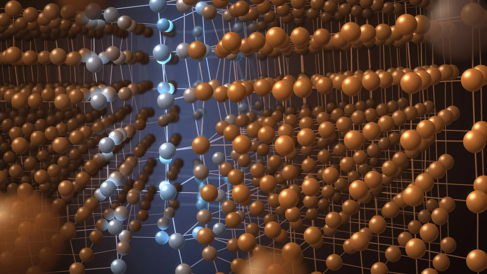
A new silicon carbide metalens with a focal length of 495μm operates at both 860nm and 1240nm wavelengths, marking a significant innovation in quantum photonic technology. Led by Xiaoying Huang and her team at the University of Technology Sydney, this metalens allows for the simultaneous capture of light from nitrogen and silicon vacancy defects within the same device, overcoming previous limitations that restricted functionality to single wavelengths.
This advancement addresses a pivotal challenge in quantum system development, where efficient manipulation and collection of light are essential. By integrating dual-wavelength functionality, researchers have created a more compact optical interface, crucial for scalable quantum applications such as secure communication and advanced computation.
Redefining Optical Systems for Quantum Applications
The dual-wavelength capability of this silicon carbide metalens effectively streamlines the optical systems required for quantum technologies. In the past, the development of quantum devices necessitated the use of separate optical components to target individual vacancies—nitrogen and silicon—complicating system design and increasing the potential for errors. With this new lens, the ability to manipulate light from both nitrogen and silicon vacancies within a single platform simplifies device architecture significantly.
Not only does this integration reduce the complexity of supporting hardware, but it also enhances performance by minimizing the space and components required. Each section of the metalens—each measuring 200×200μm—has been custom-tailored for its respective wavelength, allowing for independent phase control and efficient optical operations. With a collection half-angle estimated at about 21.8° and a numerical aperture of 0.97, it effectively captures light emissions from both defect types concurrently. This elevates the performance ceiling for quantum photonic devices and enables more sophisticated applications.
Challenges and Future Directions in Fabrication
Despite the promising applications, the team acknowledges existing challenges in achieving uniform defect placement across larger silicon carbide substrates. Variability in defect density remains a significant hurdle that researchers need to address for widespread practical application. Finding a method to maintain consistent defect characteristics will be pivotal. If you're working in this space, you know that without uniformity, scaling the technology will be troublesome at best; it's like building a house on a shaky foundation.
By developing a monolithic design capable of supporting simultaneous optically detected magnetic resonance from both types of vacancies, Huang's research significantly contributes to the quest for efficient quantum photonic systems. That said, further refinement of fabrication techniques will be essential not just to improve defect consistency, but also to enhance overall device performance. While these advancements are noteworthy, they serve as stepping stones in a journey that demands relentless innovation and scrutiny.
Implications and Future Outlook
What's at stake here isn't just an engineering marvel; these advancements could redefine what we understand about quantum technologies. The ability to control and manipulate light in novel ways opens doors to new applications in secure communication, advanced computational paradigms, and even medical imaging techniques. As industries stand on the brink of what could be a quantum revolution, devices like this metalens serve as critical enablers.
While the current challenges must be meticulously addressed, the work being done could have lasting significance in making quantum technologies more accessible. The acceptance of silicon carbide as a viable material for these purposes may lead to broader research into other non-traditional substrates, enriching the field further. Each small step forward like this one isn't just an advancement; it's a mosaic piece in a much larger picture of technological evolution.
👉 More information
🗞Engineering of Dual Wavelength, Polarization Selective Metalenses in Silicon Carbide
✍️Xiaoying Huang, Ziwei Yang, Konosuke Shimazaki, Kritsana Saego, Otto Cranwell Schaeper, Evan Williams, Dragomir Neshev, Hark Hoe Tan, Igor Aharonovicha and Mehran Kianinia
🧠 ArXiv: https://arxiv.org/abs/2608.17506

Explore more quantum computing news on Quantum Zeitgeist to keep up with the latest advancements in qubits, hardware, and algorithms.



Discussion
Sign in to join the discussion.